PCB Design & Prototyping in Kenya
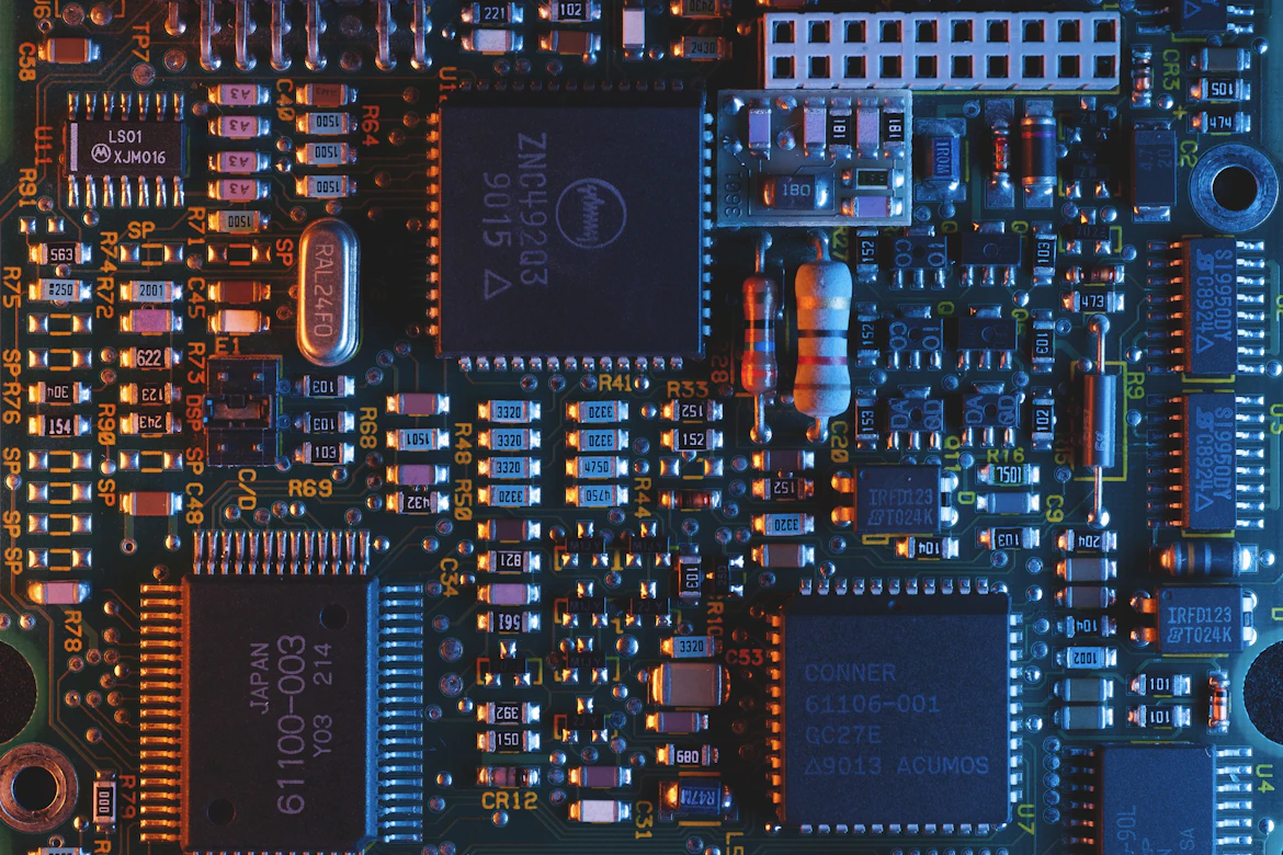
Professional PCB design and prototyping services for engineers, startups and researchers in Kenya, based at MMUST Kakamega. We turn electronic concepts into reliable hardware ready for production. What we do: schematic capture, component selection, 2‑layer and 4‑layer layout, DFM checks, thermal and signal integrity simulation, Gerber and drill file generation, bill of materials, reverse engineering, prototype assembly, functional testing, firmware integration. How it works: you provide a brief or requirements document → we create the schematic and component list → layout is performed using Altium Designer, KiCad or Eagle with design‑rule checks → a design review meeting is held → manufacturing files (Gerber, assembly drawings) are prepared and sent to our partner PCBasic for fabrication and SMT assembly → we conduct functional testing and firmware loading → the finished boards are shipped to you. Tools include simulation software, test rigs and automated assembly equipment. We operate from the Tafiti R&I Hub at MMUST Kakamega, serving Nairobi and the whole of Kenya, with support from PCBasic for PCB fabrication and MMUST/SPIIC for research incubation. Contact us today to request a quote [price: from KES X] and learn about our typical turnaround [turnaround: X days].